We are primarily interested in the synthesis and characterization of functional materials, with a focus on complex oxides (ferroelectrics, multiferroics, magnetic materials), halide perovskites, novel van der Waals (2D) and quantum materials. We have a wide variety of advanced scanning probe microscope systems in our labs to study fundamental electronic, optical and magnetic properties at the nanoscale and atomic length scales in these materials, especially those associated with interfaces and various topological structures such as domain walls, skyrmions, vortices, etc. for novel applications in nanoelectronics and quantum technology (e.g. see Seidel, Nature Materials 18, 188 (2019).
Oxides as the world’s most abundant materials are found everywhere as they make up 99% of earth’s outer crust, however their special properties at the nanoscale and atomic scale are largely unknown due to the fact that these materials are very difficult to study at these length scales. Now nanoscale oxides are roughly at the same stage of technological development as semiconductors were in the early 1970s – a period when researchers were finally learning how to work with them well enough to enable industrial applications such as the transistor and the computer.
Recent progress in oxide 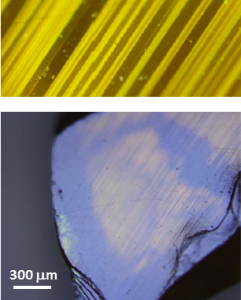 materials characterization and fabrication techniques now begin to give us a glimpse into the future for oxide nanoelectronics and progress is becoming fast-paced. Functional oxides such as ferroelectrics, multiferroics, magnetic materials are increasingly found in new electronic components, sensors, memory devices (see e.g. Science Advances 3, e1700512 (2017)), quantum technology, and in solar cells. To quote Joerg Heber, Senior Editor at the Nature Publishing Group: “The journey has merely begun”.
Organic-inorganic metal halide perovskites have gained considerable attention for next-generation photovoltaic cells due to rapid improvement in power conversion efficiencies. Our work makes use of complementary nanoscale scanning probe microscopy imaging techniques, specifically PFM, KPFM, and AFM to identify structural variations of metal halide perovskites under varying light illumination and bias conditions. Our results have provided pioneering insight into nanoscale electronic and structural variations in operating solar cells, such as those associated with grain boundaries, for improving the design of halide perovskite photovoltaic devices (e.g. see Nature Communications 10, 444 (2019).
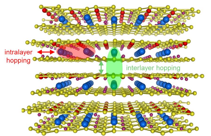
Our work on novel van der Waals (2D) materials (for 2D ferroelectrics see our recent review in Nature Reviews Materials 8, 25 (2023)) has led to the confirmation that the coexistence of reversible polar distortions and metallicity can lead to a native ferroelectric metal, which was first suggested by P. W. Anderson and E. I. Blount back in 1965. Metallicity and ferroelectricity, which usually strongly exclude each other in a material, coexist in bulk crystalline van der Waals WTe2. We show that, despite being a Weyl semimetal, WTe2 possesses switchable spontaneous polarization and a natural ferroelectric domain structure at room temperature. This new class of materials has tantalizing potential for functional nanoelectronics applications (see Science Advances 5, eaax5080 (2019).
Our current research interests and capabilities include the following:
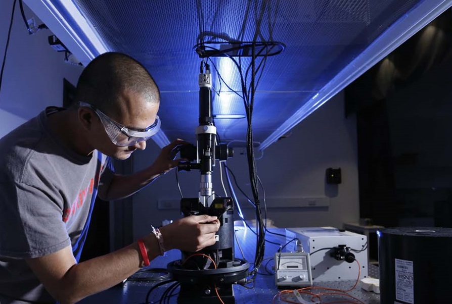
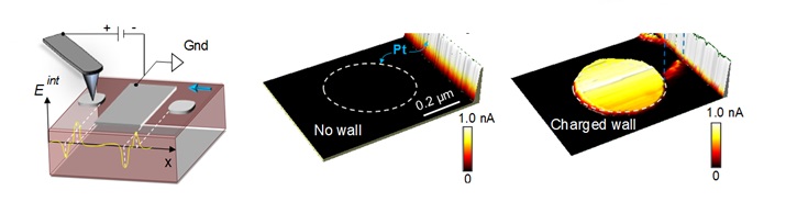
● Advanced Scanning Probe Microscopy (SPM) based Materials Characterization: We have a focus on SPM techniques to characterise material properties at the nanoscale, these include piezoresponse force microscopy (PFM), conducting-AFM (c-AFM), scanning tunneling microscopy and spectroscopy (STM/STS), Kelvin probe force microscopy (KPFM), magnetic force microscopy (MFM), quantum microscopy (NV centre SPM), scanning near-field optical microscopy (SNOM), and many more, as well as SPM instrument and methodology development (e.g. ‘crackling noise microscopy’, a new SPM technique, Nature Communications 14, 4963 (2023)). SPM measurements are performed in various sample environments, including:
- variable temperature from 3.5 to 600 Kelvin
- high magnetic field up to 9 Tesla
- measurements under light illumination (400-800nm, other wavelengths possible), with IR AFM feedback laser for solar cells (nanoscale photoconductivity and photovoltaic characterization)
- quantum microscopy using diamond NV centre SPM for nanoscale magnetic imaging
- SNOM and nano-IR imaging and spectroscopy with ~10 nm lateral resolution in the range of 550 cm-1 to 7140 cm-1, including time-resolved pump probe measurements
- protective and functional gas atmospheres (UHV, He, N2 and Ar, …)
- controllable humidity
- in-situ sample bending, stretching stages
- AFM-based nanoindentation for nanoscale mechanical characterisation, e.g. to assess elastic modulus and plastic deformation characteristics of materials with few nm lateral resolution
- high voltage application to samples during AFM measurements (e.g. for switching thicker ferroelectric ceramics and crystals)
- several of our SPM systems also allow for the study of prototype electronic device structures under operating conditions (multiple in-situ electrical contacts)
- other in-house designed instrument capability not available elsewhere (for example crackling noise microscopy, Nature Communications 14, 4963 (2023))
We are open to interesting new collaborative work involving our SPM capabilities, please contact us with details of your measurement requirements.
● Growth and Characterization of Transition Metal Oxide Thin films: We use pulsed laser deposition (PLD) techniques for high quality epitaxial thin film growth of oxides with atomic precision; X-ray diffraction for studying strain conditions and material quality, strain engineering, synthesis of artificial structures (ordered structures, superlattices, multilayers), and stabilization of metastable phases through heteroepitaxy.
●Strongly Correlated Electron Phenomena and Quantum Materials: 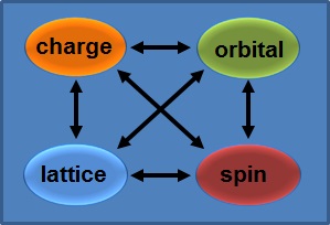 Inter-coupled phenomena of charge, spin, and orbital and lattice degrees of freedom enable new functionality in quantum materials and can lead to polar metals, metal-insulator transitions, colossal magnetoresistance, orbital/charge ordering, frustrated magnetism, and dilute magnetic semiconductors. We use transport and scanning probe measurements at variable temperatures and magnetic fields, and electric field based modulation techniques to study these phenomena.
●New Functionality in Perovskites: 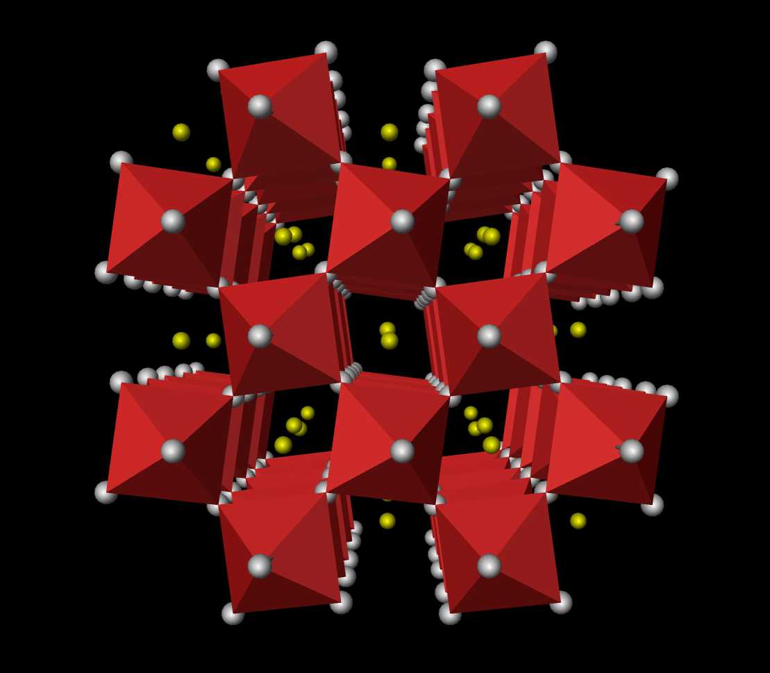 We are interested in multiferroic thin films for magnetoelectric devices and spintronic applications (complex oxide perovskites), solar energy conversion to electric power in halide perovskite materials and solar cells, non-volatile information storage, ferroelectric memory, resistive-switching memory, and electric field control of electronic conduction, ferroelectricity and magnetism.
●Materials Processing for Devices and Nanoscale Characterization: Device fabrication techniques that we use include electron-beam-lithography and etching techniques, scanning probe based lithography and others.
● Use of Large Research Facilities: We perform work at synchrotron and neutron research facilities in Australia (ANSTO), Japan (SPring-8) and Germany (BESSY, DESY). This includes nanoscale characterization of magnetic and electronic structure through state-of-the-art characterization tools such as photoemission electron microscopy (PEEM), elastic and inelastic neutron scattering, and electron microscopy to carry out element specific spectromicroscopy.