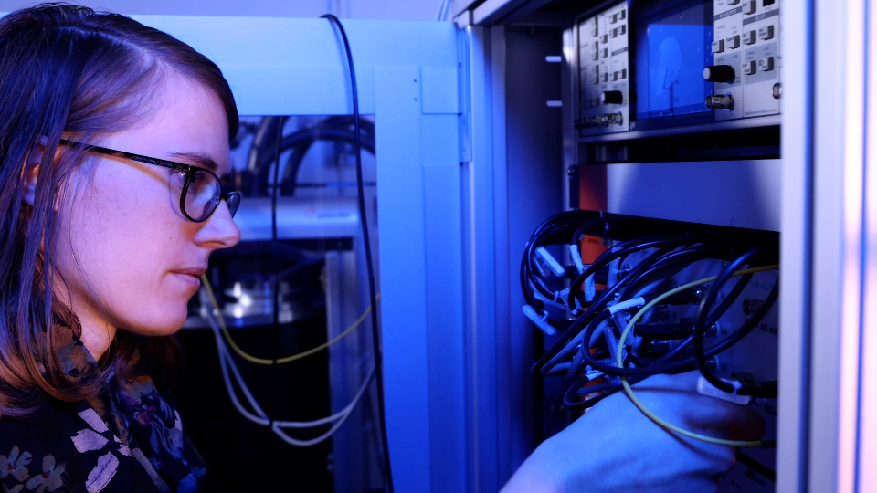
We employ several experimental techniques with a focus on advanced scanning probe microscopy (SPM) for materials characterisation in a wide range of sample environments, including variable temperatures from 3.5 to 600 Kelvin, high magnetic fields up to 9 Tesla, measurements under light illumination (400-800nm) with IR AFM feedback laser for solar cells (nanoscale photoconductivity and photovoltaic characterization), protective and functional gas atmospheres (UHV, He, N2 and Ar, …), in-situ sample bending, stretching and nanoindentation capability for nanoscale mechanical characterisation, and other techniques, including in-house designed instrument capability not available elsewhere.
In addition, we also use electron microscopy (TEM), pulsed laser deposition of thin film materials (PLD), variable temperature transport measurements, photoemission microscopy and spectroscopy (PEEM, XMCD, XMLD), neutron scattering, and optical techniques to study the properties of transition metal oxides, halide perovskites, 2D materials, and other advanced materials.
![]()
PhD scholarships are available: email Prof. Seidel with your CV to discuss in further detail about how to apply.
![]() Postdoctoral fellowships can be hosted through the ARC DECRA program, and Feodor-Lynen Fellowships of the Alexander von Humboldt Foundation. Inquire for details.
Postdoctoral fellowships can be hosted through the ARC DECRA program, and Feodor-Lynen Fellowships of the Alexander von Humboldt Foundation. Inquire for details.
