All images are © members of the Seidel Research Group and maybe reused with permission only.
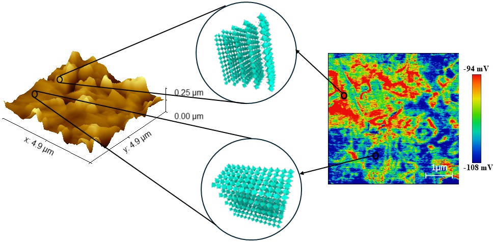
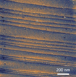
09/2024 AFM and KPFM images of a 2D polycrystalline perovskite thin film (PEA2(MA1Pb5I16) showing orientation-dependent electrical surface potentials.
– tip: Pt
– measured by Tanzeela
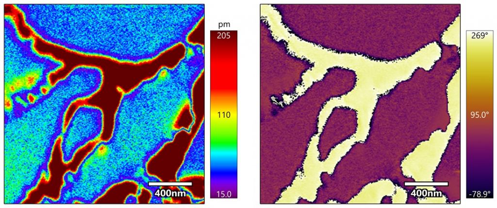
ESM image
– LiCoO2
– tip: Pt
– measured by Liang
04/2024 Electrochemical strain microscopy (ESM) image showing Li ion activity in the battery electrode material LiCoO2
SNOM image
-FAPbI3 (perovskite)
-tip: Pt
-measured by Jonghoon
04/2024 Near-field optical (SNOM ) image of a polycrystalline FAPbI3 (perovskite) sample at a characteristic mid-infrared resonance of 1710 cm-1.
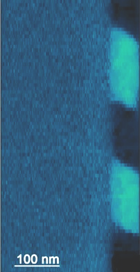
MFM image
– NbSe2
– tip: Co/Cr
– temperature: 4 K
– magnetic field: 30 mT
– dual pass lift (50 nm)
– measured by Adam
11/2022 Abrikosov vortex lattice in the type II van der Waals superconductor NbSe2
STM image
– Nb:SrTiO3, cleaved in UHV
– tip: Pt-Ir
– measured by Liang
10/2022 Unit cell terraces (3.9 Å) in UHV-cleaved niobium-doped SrTiO3
PFM amplitude and phase images
– sample: CIPS
– measured by Lei
10/2022 Nanoscale phase separation in ferroelectric copper indium thiophosphate (CIPS)
PFM phase image
– sample: BiFeO3/SrTiO3 (cross section)
– measured by Haoze
11/2022 High resolution PFM image of a FIB cross section of a BiFeO3 thin film on SrTiO3
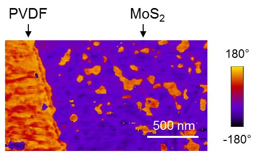
PFM phase image
– sample: MoS2 on PVDF
– measured by Dawei
11/2022 Nanoscale piezoresponse image of MoS2 on polyvinylidene fluoride (PVDF)
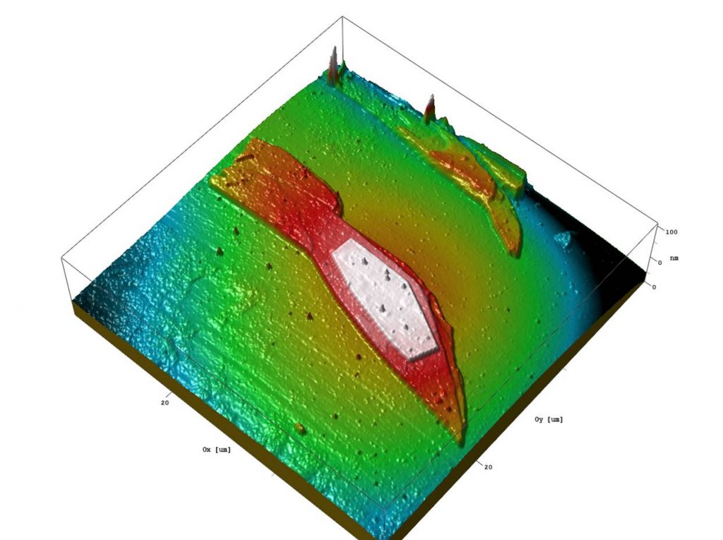
Nanostructured device imaging
– sample: WTe2 flake (red) with Pt top electrode (white)
– tip: Pt
– measured by Pankaj
07/2018 2D material flake (red) with lithographic Pt top electrode (white) on Si
PFM (Topography signal)
– sample: PMN-30%PT single crystal
– tip: Pt
– measured by Dawei
05/2018 Naturally occuring domain structure in a PMN-PT single crystal
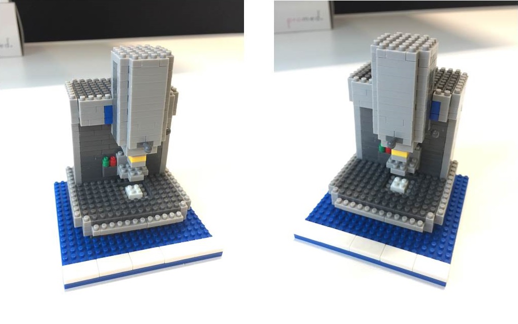
“Blocky” AFM, parts courtesy of Park Systems Inc., assembled by Fei
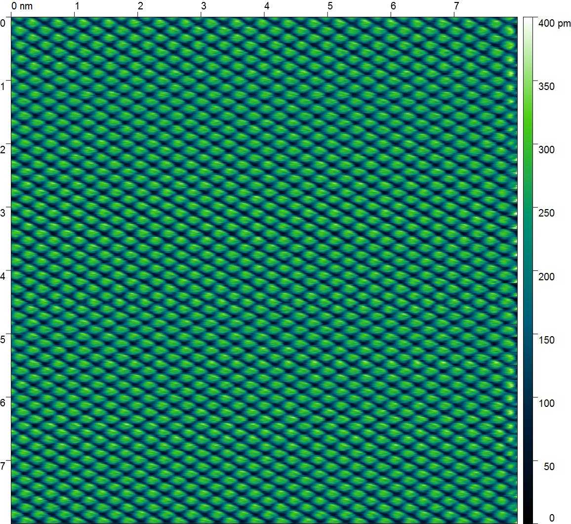
Room temperature STM
– sample: HOPG
– tip: Pt/Ir
– bias: 30mV
– tunnelling current: 0.8nA
– measured by Fei Hou
11/2017 Atomic structure of a graphite surface
Bias-assisted AFM lithography / KPFM
– sample: LaAlO3/SrTiO3
– tip: Pt
– measured by Fan Ji
10/2017 Patterned 2-DEG at LaAlO3/SrTiO3 interface seen as change in surface potential
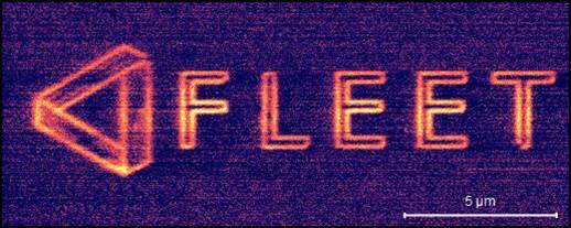
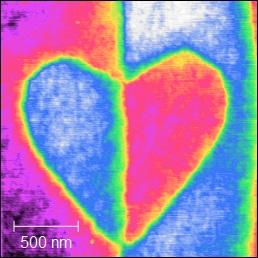
Bias-assisted vector lithography / PFM
– sample: LaAlO3/SrTiO3
– tip: Pt
– measured by Fan Ji
09/2017 FLEET logo written into 2-DEG at LaAlO3/SrTiO3 interface
MFM
– sample: SrCoO3
– tip: Co/Cr
– temperature: 3.8 K
– dual pass lift (30 nm)
– measured by Songbai Hu
09/2016 Magnetic domain structure of a SrCoO3 thin film at 3.8K
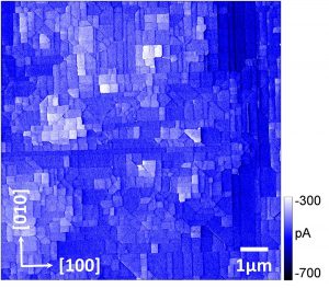
c-AFM
– sample: SrCoO3
– tip: Pt
– Vs = 1.7 V
– measured by Songbai Hu
08/2016 Conductive islands in a 40 nm thick oxidized SrCoO3 thin film on SrTiO3 (100)
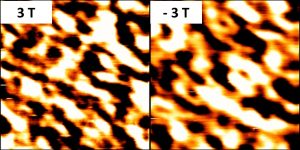
MFM
– sample: FeV2O4
– tip: Co/Cr
– temperature: 10 K
– constant height (50 nm)
– image size: 3 μm × 3 μm
– measured by Dohyung Kim
07/2016 Magnetic domain structure of an iron vanadate thin film in 3 T and -3 T magnetic fields
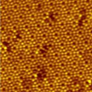
STM
– sample: Si (111) – 7 × 7
– tip: Pt/Ir on qPlus sensor
– temperature: 16 K Vs = 1.7 V, I = 0.2 nA
– image size: 20 nm × 20 nm (512 x 512)
– measured by Byoung Choi
06/2016 Atomic structure of a silicon surface
 Ferroics retreat, Kangaroo Valley 2017
 Ferroics retreat, Kangaroo Valley 2016